PRODUCT
Bonding Technology Overview
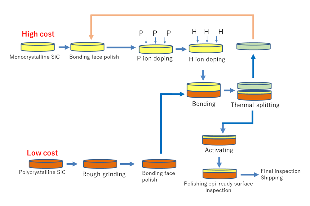
Through polishing monocrystalline and polycrystalline SiC substrates, bonding them after ion doping and then thermally splitting them, we form a thin monocrystalline layer on top of a polycrystalline substrate.
Direct Bonded Substrate Superiority
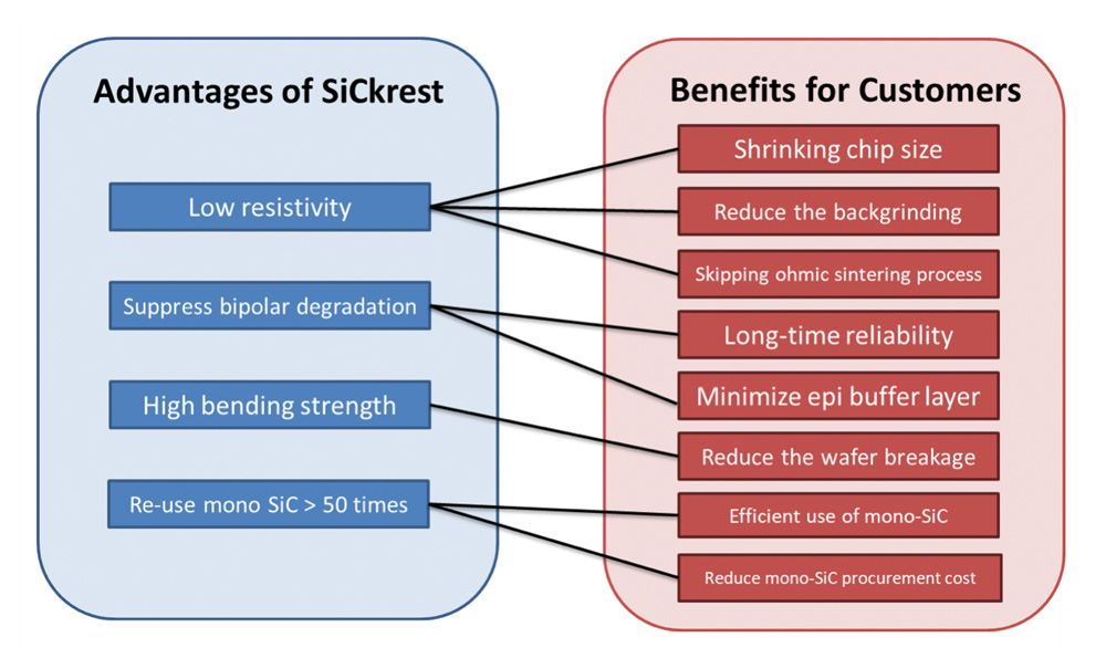
We are able to contribute to improving your products and processes through the numerous characteristics shown in the image on the right.
Reference: Presentation at 2019 Advanced Power Semiconductors Subcommittee, titled "Device characteristics of SBD with Low Cost Direct Bonding Method SiC Wafer"
Reference: Presentation at 2020 Advanced Power Semiconductors Subcommittee, titled "Annealing-free ohmic realized by bonded SiC substrate"
Reference: Presentation at 2020 Advanced Power Semiconductors Subcommittee, titled "I-V characteristics of power devices fabricated on bonded substrate of 3C-SiC poly crystal and 4H-SiC single crystal"
Reference: Presentation at 2022 Advanced Power Semiconductors Subcommittee, titled "Evaluation of Forward Bias Degradation in 4H-SiC PiN Diodes Fabricated on 4H-SiC Bonded Substrates"
Phenomena Characteristic to Direct Bonded Substrate
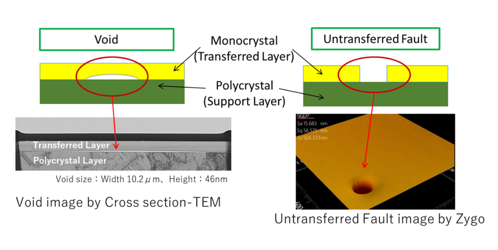
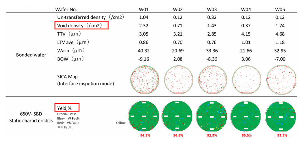
As we manufacture with a bonding process, there may be minute voids and untransferred faults (layer transfer failures) in the substrates. (See standard specifications for the guaranteed number.) Untransferred faults are killer faults as the part of these faults have no monocrystalline layer.
As in the table to the right, we measure the static characteristics of the 650V-SBD (JBS) chip and investigate the relationship between the quality characteristics of direct bonded substrates and device yield. We see no correlation between voids and SBD device yield, and we believe that the effect that voids have on device characteristics is small.
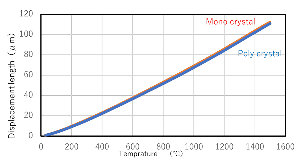
Additionally, while there may be concerns about the transferred layer peeling off, there is no variation between the monocrystalline and polycrystalline thermal expansion coefficient as shown in the graph to the right, so there will be no peeling due to thermal expansion difference.